HV5160
HV5160
1. Introduction
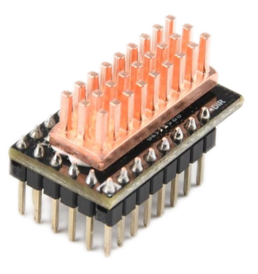
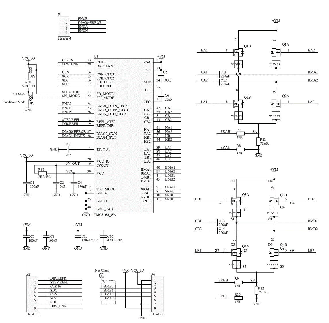
HV5160 is specially designed for high-voltage drive requirements and can work in the voltage range of 8-60V, such as 48V. The design is based on TMC5160-WA and uses Samsung Electronics’ 100V X7R ceramic capacitors
2. Feature
- 1000 x 600mil / 25.4 x 15.24mm
- 6 layer TG155 PCB
- 8-60V 3.0A (rms) / 4.2A (peak)
- 4x DMT6018 (17 mΩ)
- Step/Dir interface & SPI mode default
- Compatible with Stepstick Pins
- Encoder Interface pinout
- DIAG output for sensorless homing
- With 393.6 W/(m·K) copper heatsink
3. Application
3D printers, CNCs, engraving machines, or other similar devices with stepper motors.
4. Specifications
Items | TMC5160 | HV5160 |
|---|---|---|
Motor Voltage (VM) | 8-40V | 8-60V |
Size | 800 x 600mil / 20.32 x 15.24mm | 1000 x 600mil / 25.4 x 15.24mm |
MOSFET | 4x WSD4066 (17mΩ) | 4x DMT6018 (17 mΩ) |
Heatsink | 238.6 W/(m·K)铝散热片 | 393.6 W/(m·K)纯铜散热片 |
Motor Phase Current max | 3.0A (rms) / 4.2A (peak) | |
Rs | 0.075Ω | |
Default Mode | SPI Mode,Standalone mode selectable via solder option | |
PCB layer | 6层,TG155 | |
Pinout | DIAG0 & Encoder Interface pinout | |
Native Microsteps | up to 1/256 | |
microPlyer Microsteps | 1/256 | |
Logic Voltage (VIO) | 3-5V | |
Internal V-Regulator | enabled | |
stealthChop (quiet) | yes | |
spreadCycle | yes | |
coolStep | yes | |
stallGuard | yes | |
dcStep | yes |
5. Hardware Guide
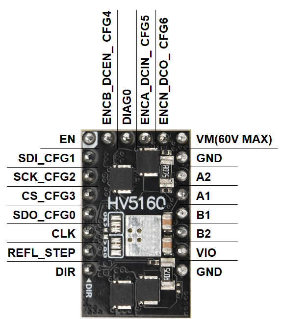
5.1 Pin Functions
Pin | Function |
|---|---|
Power Supply | |
GND | Ground |
VM | Motor Supply Voltage, Provide filtering capacity near pin with short loop to GND plane. Must be tied to the positive bridge supply voltage. |
VIO | 3.3V to 5V IO supply voltage for all digital pins. |
Motor Outputs | |
B1 | Motor Coil 1 |
B2 | Motor Coil 1 |
A1 | Motor Coil 2 |
A2 | Motor Coil 2 |
Control Inputs | |
REFL_STEP | STEP input when (SD_MODE=1).or left reference input (for internal ramp generator) |
REFR_DIR | DIR input (SD_MODE=1).or right reference input (for internal ramp generator) |
TMC5160 | |
EN | Enable Motor inputs: GND=on, VIO=off |
CLK | CLK input. Tie to GND using short wire for internal clock or supply external clock. Internal clock-fail over circuit protects against loss of external clock signal. |
SDI_CFG1 | SPI data input (SPI_MODE=1) or |
SCK_CFG2 | SPI serial clock input (SPI_MODE=1) or |
CSN_CFG3 | SPI chip select input (negative active) (SPI_MODE=1) or |
SDO_CFG0 | SPI data output (tristate) (SPI_MODE=1) or |
DIAG0 | Diagnostics output DIAG0. |
ENC-BENCB_DCEN_ CFG4 | Encoder B-channel input (when using internal ramp generator) or |
ENC-AENCA_DCIN_ CFG5 | Encoder A-channel input (when using internal ramp generator) or |
ENC-NENCN_DCO_ CFG6 | Encoder N-channel input (SD_MODE=0) or |
5.2 Configuration Instructions
If you use 48V to power the VMOT of the module and 24V step-down to power the VIO, please make sure that 48V and 24V are turned on at the same time (that is, VMOT and VIO arrive at the same time). Otherwise, the drive module may burn out.5.2.1 Solder Jumper
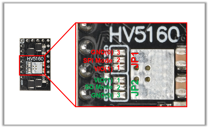
JP1SPI_MODEPin22 Integrated pull down resistor. | JP2 SD_MODEPin21 | Mode |
|---|---|---|
0 | 1 | **Standalone Mode,Step-DIR Interface,CFG pins config:**Default Mode,SPI Mode,Step-DIR Interface:The STEP/DIR inputs control the driver the chip is in standalone mode and pins have their CFG functions. |
0 | 0 | The internal ramp generator generates step pulses,enable UART operation(but the DIAG1_SWP doesn't pinout,can't use the UART interface) |
1 | 1 | **(Default)SPI Mode,Step-DIR Interface:**The STEP/DIR inputs control the driver the SPI interface is enabled. Integrated pull down resistor. |
1 | 0 | The internal ramp generator generates step pulses, the SPI interface is enabled. |
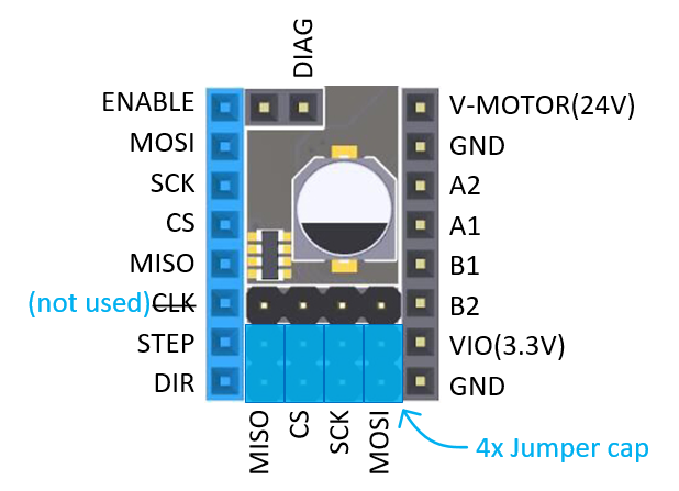
5.2.2 USE SPI mode on FYSETC Boards
6. Part List
- HV5160 x1
- Copper Heatsink x1
7. Documentations
TMC5160 Chip Datasheet
Schematic
3D mode
8. Where to buy
9. Tech Support
Please submit any technical issue into our forum ,github,facebook。
Updated on: 03/08/2026
Thank you!